Fabrication
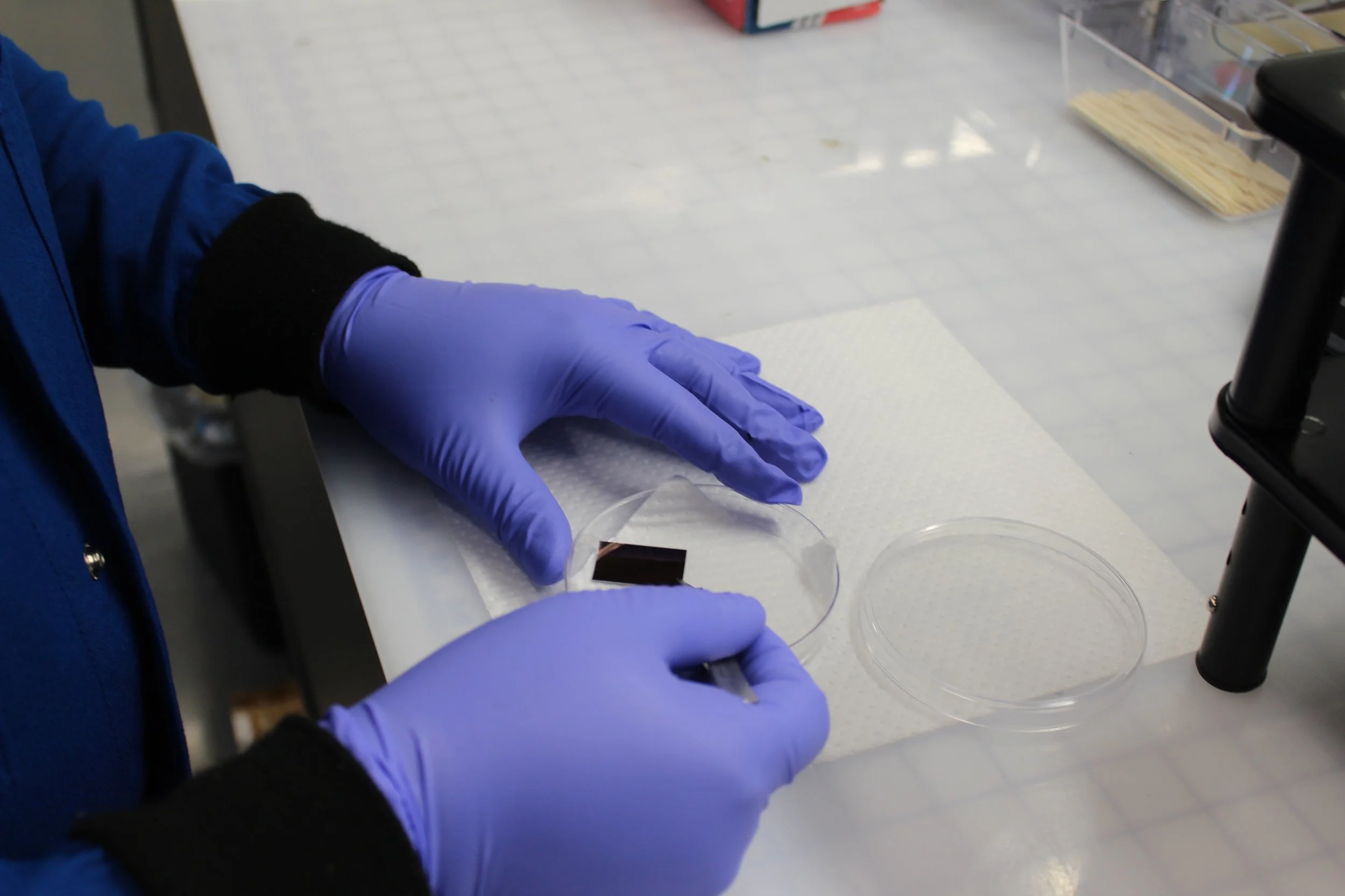
Nanofabrication is the process of engineering structures, circuits, and electrical contacts at the nanometer scale—often thousands of times thinner than a human hair—on two-dimensional (2D) quantum materials. By combining precision lithography, thin-film deposition, and cleanroom packaging, the MonArk Quantum Foundry transforms raw layered materials into functional, testable quantum devices.
Nanofabrication process
-
Substrates are cleaned and spin-coated with a bilayer resist stack to prepare the surface for high-resolution patterning.
-
Sub-micron device features are patterned directly onto the sample using thermal scanning probe lithography (t-SPL).
Larger contact pads and interconnects are written using maskless direct-write laser photolithography.
The exposed resist layers are chemically developed and rinsed to reveal the device pattern prior to material deposition.
-
Samples undergo in-situ argon ion milling for surface cleaning or etching, followed by thin-film deposition via multi-pocket e-beam evaporation, RF/DC sputtering, or Atomic Layer Deposition (ALD).
-
Excess metal and underlying resist are removed via solvent lift-off, and the patterned structures are verified under an optical microscope.
-
Finished chips are mounted onto sample carriers and connected via a wire bonding.
Lithography Tools
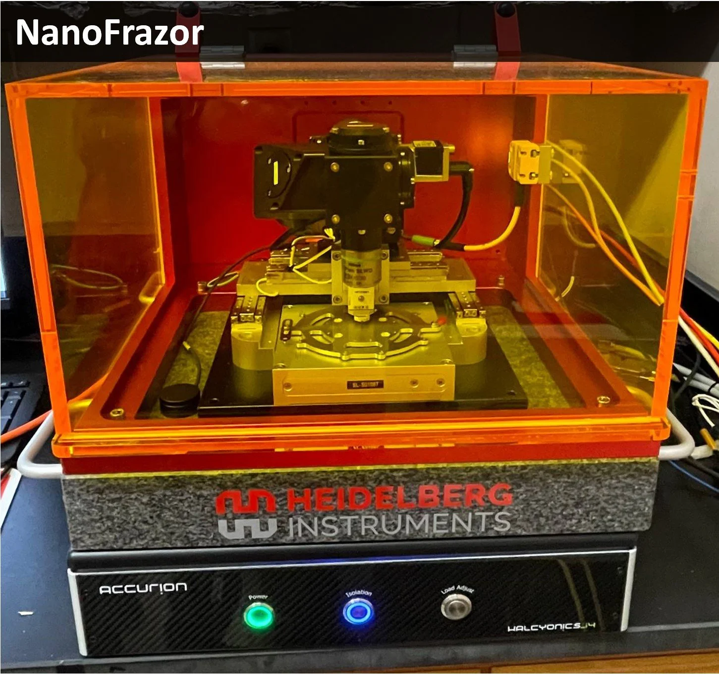
NanoFrazor
The NanoFrazor system is a state-of-the-art nanopatterning tool based on local thermal evaporation of the thermal resist using the tip of an AFM. A current is applied to locally heat the AFM tip and transfer heat to the PPA layer and sublimate this layer, making a nanopattern. The resolution of this technique is 50 nm. The system is small in size, compact, and robust to incorporate inside a glove box to fabricate nanodevice of air-sensitive materials.
µMLA
µMLA -micron photolithography tool uses a 365nm LED to pattern a photosensitive resist. LED is mounted on a moving head which rasters over the sample to generate the desired pattern without the need for any mask. The resolution of this tool is 600nm. uMLA has a fast writing speed of 10mm2/min.
Etching Tools
Xactix
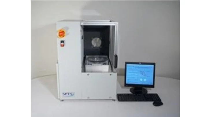
Xactix is a dry etching tool that uses various process gases to etch metal, semiconductor, and dielectric materials. The tool allows good control of etching rate as well as the selectivity of the etching material.
RIE
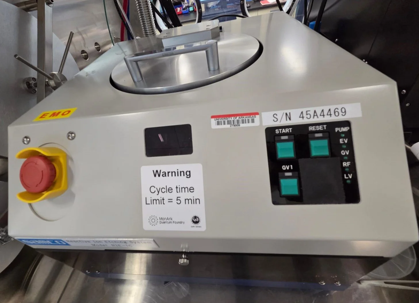
The RIE-1C is a compact, desktop dry etching system designed for convenient and reliable operation in laboratory environments. It offers a simple workflow where the etching process can be initiated at the push of a button after the sample is loaded. The system supports etching with gases including SF₆, CH₃, CH₄, and O₂, enabling versatile processing for a range of materials. It accommodates samples up to 4-inch diameter, making it suitable for small-scale research and device fabrication.
Deposition & Metallization Tools
AJA
AJA thin film deposition tool is a high vacuum system that can deposit thin films with two different methods., namely Sputtering and electron beam (e-beam) deposition. Sputtering of various elemental films can be performed using 2 RF and 2 DC sputtering guns. The e-beam system has 6 pocket crucibles. In addition to thin film deposition, the system also consists of argon ion milling capability to clean or etch in situ.
Packaging Tools
Xactix
Xactix is a dry etching tool that uses various process gases to etch metal, semiconductor, and dielectric materials. The tool allows good control of etching rate as well as the selectivity of the etching material.
Wire Bonder
AJA thin film deposition tool is a high vacuum system that can deposit thin films with two different methods., namely Sputtering and electron beam (e-beam) deposition. Sputtering of various elemental films can be performed using 2 RF and 2 DC sputtering guns. The e-beam system has 6 pocket crucibles. In addition to thin film deposition, the system also consists of argon ion milling capability to clean or etch in situ.
RIE
The RIE-1C is a compact, desktop dry etching system designed for convenient and reliable operation in laboratory environments. It offers a simple workflow where the etching process can be initiated at the push of a button after the sample is loaded. The system supports etching with gases including SF₆, CH₃, CH₄, and O₂, enabling versatile processing for a range of materials. It accommodates samples up to 4-inch diameter, making it suitable for small-scale research and device fabrication.